- 您现在的位置:买卖IC网 > Sheet目录2005 > LTC2175IUKG-14#TRPBF (Linear Technology)IC ADC 14BIT 125MSPS QUAD 52QFN
LTC2175-14/
LTC2174-14/LTC2173-14
24
21754314fa
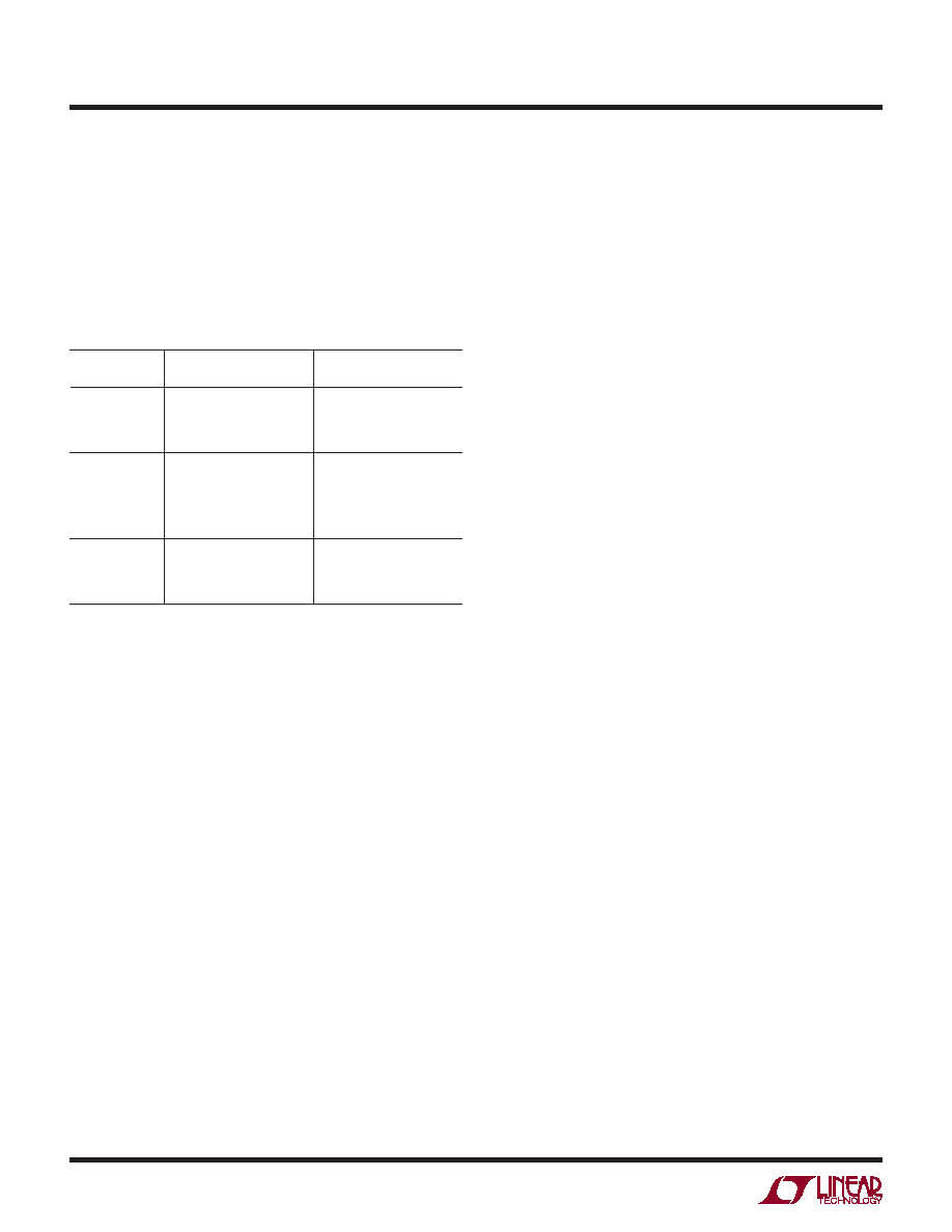
Table 2. Output Codes vs Input Voltage
AIN+ – AIN–
(2V RANGE)
D13-D0
(OFFSET BINARY)
D13-D0
(2’s COMPLEMENT)
>1.000000V
+0.999878V
+0.999756V
11 1111 1111 1111
11 1111 1111 1110
01 1111 1111 1111
01 1111 1111 1110
+0.000122V
+0.000000V
–0.000122V
–0.000244V
10 0000 0000 0001
10 0000 0000 0000
01 1111 1111 1111
01 1111 1111 1110
00 0000 0000 0001
00 0000 0000 0000
11 1111 1111 1111
11 1111 1111 1110
–0.999878V
–1.000000V
<–1.000000V
00 0000 0000 0001
00 0000 0000 0000
10 0000 0000 0001
10 0000 0000 0000
applicaTions inForMaTion
DATA FORMAT
Table 2 shows the relationship between the analog input
voltage and the digital data output bits. By default the
output data format is offset binary. The 2’s complement
format can be selected by serially programming mode
control register A1.
and all other bits. The FR and DCO outputs are not affected.
Theoutputrandomizerisenabledbyseriallyprogramming
mode control register A1.
Digital Output Test Pattern
To allow in-circuit testing of the digital interface to the
A/D, there is a test mode that forces the A/D data outputs
(D13-D0) of all channels to known values. The digital
output test patterns are enabled by serially programming
mode control registers A3 and A4. When enabled, the test
patterns override all other formatting modes: 2’s comple-
ment and randomizer.
Output Disable
Thedigitaloutputsmaybedisabledbyseriallyprogramming
mode control register A2. The current drive for all digital
outputs including DCO and FR are disabled to save power
or enable in-circuit testing. When disabled the common
mode of each output pair becomes high impedance, but
the differential impedance may remain low.
Sleep and Nap Modes
The A/D may be placed in sleep or nap modes to conserve
power. In sleep mode the entire chip is powered down, re-
sultingin1mWpowerconsumption.Sleepmodeisenabled
by mode control register A1 (serial programming mode),
or by SDI (parallel programming mode). The amount of
time required to recover from sleep mode depends on the
size of the bypass capacitors on VREF, REFH, and REFL.
For the suggested values in Figure 8, the A/D will stabilize
after 2ms.
In nap mode any combination of A/D channels can be
powered down while the internal reference circuits and the
PLL stay active, allowing faster wakeup than from sleep
Digital Output Randomizer
Interference from the A/D digital outputs is sometimes
unavoidable.Digitalinterferencemaybefromcapacitiveor
inductive coupling or coupling through the ground plane.
Even a tiny coupling factor can cause unwanted tones
in the ADC output spectrum. By randomizing the digital
output before it is transmitted off chip, these unwanted
tones can be randomized which reduces the unwanted
tone amplitude.
The digital output is randomized by applying an exclusive-
OR logic operation between the LSB and all other data
output bits. To decode, the reverse operation is applied
—an exclusive-OR operation is applied between the LSB
发布紧急采购,3分钟左右您将得到回复。
相关PDF资料
LTC2202IUK#TRPBF
IC ADC 16-BIT 10MSPS 48-QFN
LTC2205IUK-14#PBF
IC ADC 14BIT 65MSPS 48-QFN
LTC2207IUK-14#PBF
IC ADC 14BIT 105MSPS 48-QFN
LTC2220IUP-1#TRPBF
IC ADC 12BIT 185MSPS 64-QFN
LTC2221IUP#TRPBF
IC ADC 12-BIT 135MSPS 64-QFN
LTC2222IUK-11#TRPBF
IC ADC 11BIT 105MSPS SAMPL 48QFN
LTC2223IUK#TRPBF
IC ADC 12BIT 80MSPS SAMPLE 48QFN
LTC2224IUK#TRPBF
IC ADC 12BIT 135MSPS SAMPL 48QFN
相关代理商/技术参数
LTC2175IUKG-14PBF
制造商:LINER 制造商全称:Linear Technology 功能描述:14-Bit, 125Msps/105Msps/80Msps Low Power Quad ADCs
LTC2175IUKG-14TRPBF
制造商:LINER 制造商全称:Linear Technology 功能描述:14-Bit, 125Msps/105Msps/80Msps Low Power Quad ADCs
LTC2180
制造商:LINER 制造商全称:Linear Technology 功能描述:12-Bit, 65Msps/ 40Msps/25Msps Low Power Dual ADCs
LTC2180CUP#PBF
制造商:Linear Technology 功能描述:ADC Dual 25Msps 16-bit Parallel/Serial (SPI)/LVDS 64-Pin QFN EP 制造商:Linear Technology 功能描述:IC ADC 16BIT DUAL PAR/SRL 64QFN 制造商:Linear Technology 功能描述:ADC 2CH 16BIT 25MSPS QFN-6 制造商:Linear Technology 功能描述:ADC, 2CH, 16BIT, 25MSPS, QFN-64 制造商:Linear Technology 功能描述:ADC, 2CH, 16BIT, 25MSPS, QFN-64; Resolution (Bits):16bit; Sampling Rate:25MSPS; Supply Voltage Type:Single; Supply Voltage Min:1.7V; Supply Voltage Max:1.9V; Supply Current:43.5mA; Digital IC Case Style:QFN; No. of Pins:64 ;RoHS Compliant: Yes
LTC2180CUP#PBF-ES
制造商:Linear Technology 功能描述:ADC Dual 25Msps 16-bit Parallel/Serial (SPI)/LVDS 64-Pin QFN EP
LTC2180CUP#TRPBF
制造商:Linear Technology 功能描述:ADC Dual 25Msps 16-bit Parallel/Serial (SPI)/LVDS 64-Pin QFN EP T/R 制造商:Linear Technology 功能描述:IC ADC DUAL 16BIT 25MSPS 64-QFN
LTC2180CUP#TRPBF-ES
制造商:Linear Technology 功能描述:ADC Dual 25Msps 16-bit Parallel/Serial (SPI)/LVDS 64-Pin QFN EP T/R
LTC2180IUP#PBF
制造商:Linear Technology 功能描述:ADC Dual 25Msps 16-bit Parallel/Serial (SPI)/LVDS 64-Pin QFN EP 制造商:Linear Technology 功能描述:IC ADC 16BIT DUAL PAR/SRL 64QFN